Precision Measuring Instrument Solutions Semiconductor Industry Edition
Responding to the increasingly sophisticated production lines of the semiconductor industry
The semiconductor industry supports cutting-edge technologies such as EVs, autonomous driving, and the fifth-generation mobile communication system (5G). We offer effective precision measuring equipment solutions for semiconductor production lines, which require high levels of precision, quality, and productivity.
Semiconductor front-end applications
- Ingot outer diameter
- A/N MARK (SEMI standard): Width, position, dot diameter and depth
- Exposure device control
- CVD equipment parts: ceramic heaters, silicon rings (flatness, cross-sectional shape analysis, surface roughness)
- CVD equipment parts: shower head nozzle hole (inner diameter, roundness, position accuracy)
- Wafer Thickness
- CMP equipment parts: polishing pads (groove width, groove depth, groove pitch, surface roughness)
- Etching equipment parts: electrostatic chucks, silicon rings (flatness, cross-sectional shape, surface roughness)
- Etching equipment parts: shower head nozzle hole (inner diameter, roundness, position)
- Probe cards, IC test sockets (pin height, holes)
- Wafer prober, probe needle
Semiconductor back-end applications
- Cutting surface observation
- Chip Thickness
- Burr height on the back side after cutting
- Lead frame (width, pitch, height, twist, etc.)
- Wire Loop Height
- Lead width, pitch, height variation, gap
- Solder ball height, diameter and pitch
- Package Substrate Coplanarity
Related products

QV HYBRID TYPE4 series Vision Measuring System equipped with non-contact displacement sensor For measuring the flatness, cross-sectional shape, surface roughness, etc. of silicon rings

General-purpose Vision Measuring System(high-spec model) QUICK VISION Apex series For measuring A/N MARK width, position, dot diameter, depth, etc.

Contour Measuring Machine For measuring roughness of the back surface of a wafer, surface roughness of a polishing pad, etc.

Measuring Microscope For measuring holes in IC test sockets, wear probes, probe needles, lead frames, etc.

High-accuracy Non-contact In-line
Measuring System/Laser Scan Micrometers For measuring the outer diameter of ingots, lead width, pitch, gap, etc.

High-precision linear gauge LGH For measuring the thickness of wafers and chips

Control linear scale (linear encoder) For controlling exposure equipment, etc.
Related inquiries/FAQ
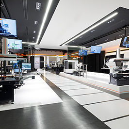
Information on the showroom where you can actually see and experience Mitutoyo products and technologies.
Mitutoyo has deployed M3 Solution Centers around the world as demonstration spaces to demonstrate and propose Mitutoyo products and solutions. In addition to product exhibitions and demonstrations and practical guidance from full-time engineers, we also offer consultation on system implementation.
Learn more about M3 Solution Center